DC lab4和lab6略解
本文最后更新于:2022年10月19日 下午
本文记录了DC LAB4和LAB6实验,表达了个人的一些见解,包括详细的计算方法。
由于LAB4和LAB6涉及均是很基础的约束设计,且笔者主要跑流程,并未对相关的概念细节和设置进行深究,敬请谅解。
1. 面积约束
【代码】
1 | |
2. 时序约束
2.1 总论
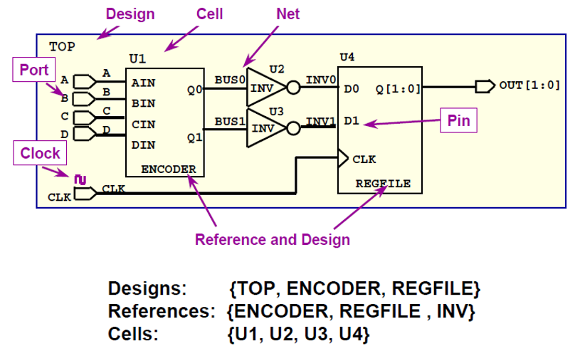
1. 设计对象
设计对象分类(8种):
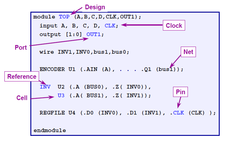
- 设计(design):顶层模块(TOP module)
- 单元(cell):各种例化的模块
- 引用(reference):例化单元的原模块(库)
- 端口(port):模块(TOP module)的输入(input)、输出(output)等
- 引脚(pin):模块中,例化单元的各个接口
- 连线(net):模块中用于将端口和引脚、或引脚和引脚互连起来的导线
- 时钟(clock):模块中的时钟端口(port)或者引脚(pin)
- 库(library)
【注意】
- 以上的区分并不准确,主要需要理解的是【port】、【pin】、【clock】
- 在设计中,时钟端口的声明和其他普通输入输出的端口并没有区别;时钟端口是在约束文件中进行具体声明,同其他普通端口进行区分的
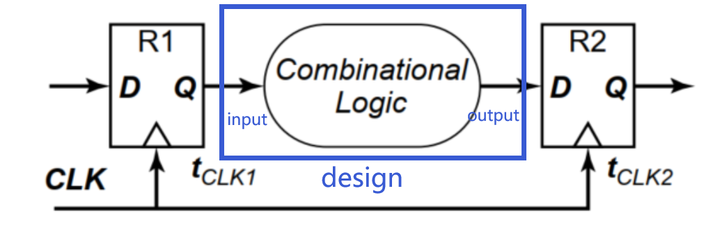
2. 四种时钟路径
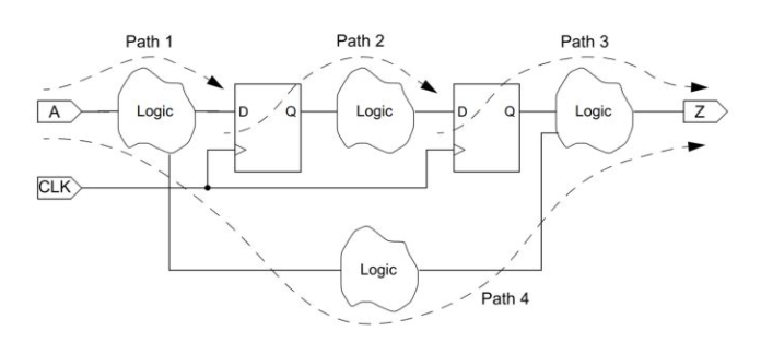
每条路径从时序路径起点开始,经过一些组合逻辑,然后在终点被捕获:
- Path 1:从输入端口开始,到达时序元件的数据输入。即(input-to-register)
Path 2:从时序元件的时钟引脚开始,到时序元件的数据输入。即(register-to-register)
Path 3:从时序元件的时钟引脚开始,到输出端口结束。即(register-to-output)
Path 4:从输入端口开始,到输出端口结束。即(input-to-output)
本次实验中,将分别对四种时钟路径进行时序约束
2.2 整体时序约束和r-to-r约束
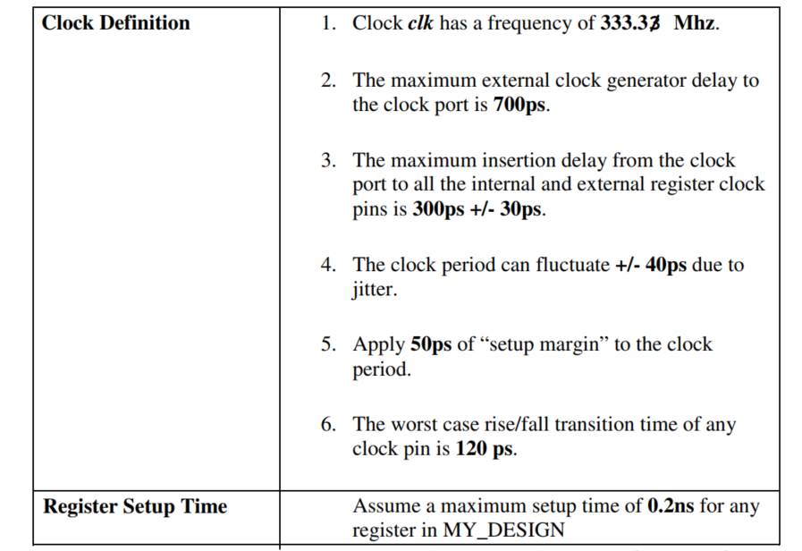
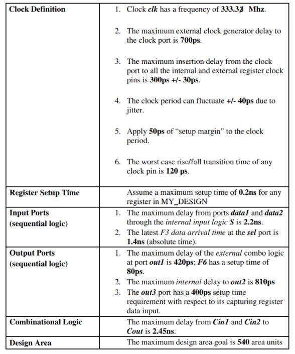
1. 时钟定义
【题目1.1】时钟频率为333.33$Mhz$:
【解析】时钟的周期为
【代码】
1
2
3
4create_clock -period 3.0 [get_ports clk]
#在端口clk产生时钟,即设置clk端口为时钟端口
#产生周期为3.0ns的时钟
【题目1.2】外部时钟产生器到时钟端口(port)的最大延迟为700$ps$
【解析】源时钟延迟,即
source_latency=700ps=0.7ns。 源时钟延迟如下图所示。
【代码】
1
2
3set_clock_latency -source -max 0.7 [get_clocks clk]
#时钟端口的源时钟延时为0.7ns
【题目1.3】从时钟端口(port)到所有内部和外部寄存器时钟引脚(pin)的最大延迟为$300±30ps$
【解析】时钟网络延时,即network latency=300ps=0.3ns。 时钟网络延时如下图所示。
存在时钟偏差(shew)
时钟偏差属于时钟不稳定(uncertainty),后文说明。
【代码】
1
2
3
4set_clock_latency -max 0.3 [get_clocks clk]
#时钟网络延迟为0.7ns
#对比源时钟延迟,少了 -source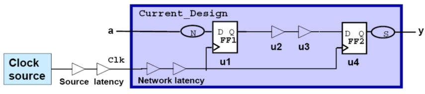
【题目1.4】略。时钟抖动(jitter)属于时钟不稳定,后文说明。
【题目1.5】略。建立时间裕量(setup margin)属于时钟不稳定,后文说明。
【题目1.6】时钟引脚(pin)在最坏情况下,上升时间和下降时间是$120ps$
【解析】无
【代码】
1
set_clock_transition 0.12 [get_clocks clk]
2. pre-CTS setup 时钟不确定性(uncertainty)
公式:
【注】:
- 此处的公式是前-时钟树综合:Clock Tree Synthesis (CTS)的建立时间不确定公式。适用于DC lab4。
时钟偏差(skew)
【题目1.3】从时钟端口(port)到所有内部和外部寄存器时钟引脚(pin)的最大延迟为$300±30ps$
【解析】存在时钟偏差(shew) 如下图所示,寄存时钟引脚的$±30ps$内部时钟偏差变化会导致$-60ps$的最坏情况偏斜
即,晚启动($+30ps$)和早捕获($-30ps$)
即,
|skew|=|-60ps|=0.06ns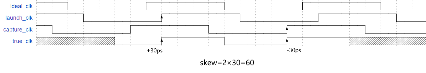
【代码】
1
set_clock_uncertainty -setup 0.06 [get_clocks clk]
时钟抖动(jitter)(具体还不好理解,目前知道考虑单倍即可)
【题目1.4】由于时钟抖动,时钟周期存在±40ps的不确定性
【解析】存在时钟抖动(jitter)
一般情况下,jitter指的是cycle_to_cycle jitter = T2 -T1、 T3-T2 …. 即两个相邻周期的差值。
最坏情况下,$|jitter|=|-40ps|=0.04ns$
【代码】
1
set_clock_uncertainty -setup 0.04 [get_clocks clk]
建立时间裕量(setup margin)
【题目1.5】每个时钟周期需要$50ps$的建立时间裕量
【解析】无
【代码】
1
set_clock_uncertainty -setup 0.05 [get_clocks clk]
【总结】:
于是代码如下:
1 | |
【注】:
时钟不确定性均是考虑最坏情况,即当前所设置的时钟周期下,由于不确定性导致了实际的时钟周期短于所设置的时钟周期,但是logic依然需要在比所设置的时钟周期的实际时钟周期内完成其运算。因为如果完不成其逻辑运算,意味着需要增大我们所设置的时钟周期,这是我们所不希望看到的。
什么时候考虑uncertainty?
答:当题目给出设计(design)内部的组合逻辑的最值时,我们需要考虑uncertainty。根据uncertainty得到实际的时钟周期$T’$,从而约束端口的时序。
如:问题4.2,out2端口内部组合逻辑的最大传播延时为$810ps$;问题5.0,Cin1和Cin2端口到Cout端口的最大延时为$2.45ns$(port-to-port,是纯组合逻辑,即内部组合逻辑的最大传播延时为$2.45ns$)。
skew和jitter:
在时序约束的时候,我们均是以【周期period】为视角,讨论如何在固定的周期内,让逻辑(logic)运算可以满足(逻辑综合,主要就是优化这些组合逻辑)。
对于skew,由于latency的不确定性,使得时钟沿到来产生了不确定性。而对于一个周期,是由两个时钟沿的,于是我们需要综合考虑两个时钟沿对于实际时钟(practical clock)的影响。最坏情况下,晚launch 30 早capture 30,周期变短$60ps$。
对于jitter,jitter的定义有很多,包括cycle-to-cycle 、Period-jitter。此处指的是cycle-to-cycle,即$±40ps$就是周期级别的不稳定性了。
2.3 输入时序约束(i-to-r)
1. 计算方法
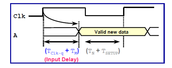
input-to-register 需要自己构造 外部的逻辑(external logic),我们需要计算出【input delay】来约束输入端口的时序。
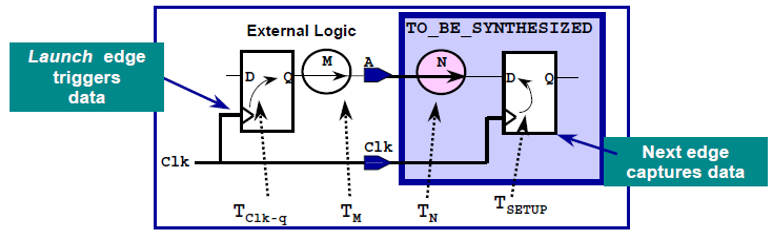
令,input delay
其中,
$T_{Clk-q}$:外部电路寄存器的传播延时
$T_M$:外部组合逻辑电路的最坏传播时间
如下图,
2. LAB解读
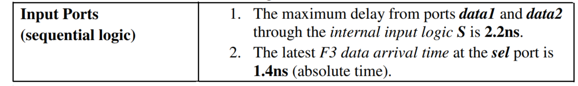
【题目3.1】从端口data1和data2通过内部逻辑S的到达寄存器R1、R2的延时为$2.2ns$
【解析】由题可知,$T_N=2.2ns$
“走”的时间$T=T_{Clk-q}+T_M+T_N=input\ delay +T_N$
“允许”的时间$T_允=T-uncertainty-T_{setup}$
需要满足$T_走≤T_允$,即$input\ delay <T-uncertainty-T_{setup}-T_N$
即,$input\ delay=3-0.15-0.2-2.2=0.45ns$
【代码】
1
2
3set_input_delay -max 0.45 -clock clk [get_ports data*]
#注意,此处是对输入的一些特定端口(special port)进行约束,故[get_ports data*]
【题目3.2】F3的数据到达
sel的绝对时刻是$1.4ns$时刻【解析】F3的数据到达
sel的绝对时刻是$1.4ns$时刻,即在$ideal \ clock$对应的$t=1.4ns$时,数据就要到达sel端口(port) 但是F3的时钟同样存在latency,如下图。
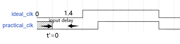
source_latency和network_latency加起来,总的latency为$1ns$,即当$t’=0$时,$ideal \ clock$对应的$t=1ns$
因此$input\ delay=absolute\ time-latency=1.4-1=0.4ns$
【代码】
1
set_input_delay -max 0.4 -clock clk [get_ports sel]
2.4 输出时序约束(r-to-o)
1. 计算方法
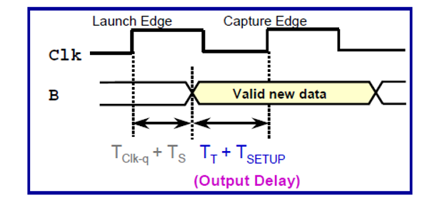
register-to-output 需要自己构造 外部的逻辑(external logic),我们需要计算出【output delay】来约束输出端口的时序。
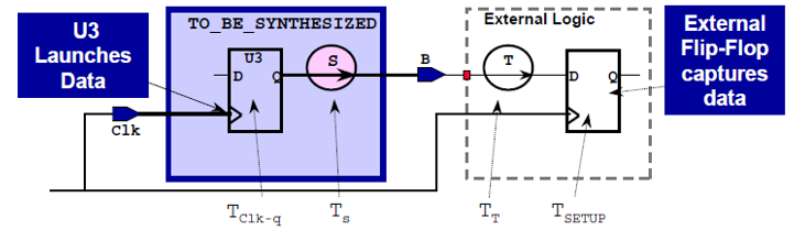
令,output delay
其中,
$T_T$:外部组合逻辑的最大传播延时
$T_{SETUP}$:外部所构造的capture寄存器的建立时间
如下图:
2.LAB解读
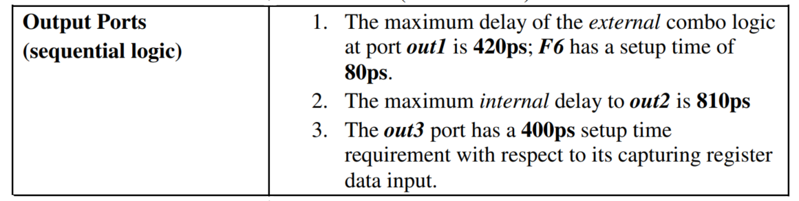
【问题4.1】out1端口外部组合逻辑的最大传播延时为$420ps$,F6的建立时间为$80ps$
【解析】外部组合逻辑的最大传播延时$T_=420ps=0.42ns$
外部所构造的capture寄存器的建立时间$T_{SETUP}=80ps=0.08ns$
于是,$output\ delay = T_T+T_{SETUP}=0.42+0.08=0.5ns$
【代码】
1
set_output_delay -max 0.5 -clock clk [get_ports out1]
【问题4.2】out2端口内部组合逻辑的最大传播延时为$810ps$
【解析】注意,此处涉及到内部组合逻辑,计算output delay需要构造如下图所示的内外部电路
因为涉及到内部电路,故还需要考虑uncertainty
由题可知,$T_S=810ps=0.81ns$
根据定义,理想条件下,$T=T_{Clk-q}+T_S+T_T+T_{SETUP}$(具体见数集(10))
由于条件中,$T_{Clk-q}$未给出,可令为0;$output\ delay = T_T+T_{SETUP}$
于是,$T=T_S+output\ delay$
由于涉及到内部的寄存器,故需要考虑uncertainty,即
$T’=T-uncertainty=3-0.15=2.85ns$
要让时序满足,则$T_S+output\ delay≤T’$,于是$output\ delay=T’-T_S=2.85-0.81=2.04ns$
【代码】
1
set_output_delay -max 2.04 -clock clk [get_ports out2]
【问题4.3】out3端口外的capture寄存器需要$400ps$的建立时间
【解析】根据电路图,out3端口外无组合逻辑电路,即$T_T=0$
于是,于是,$output\ delay = T_T+T_{SETUP}=0+400ps=0.4ns$
【代码】
1
set_output_delay -max 0.4 -clock clk [get_ports out3]
2.5 input-to-output时序约束
1. 计算方法
input-to-output 时钟路径采用如下模型,我们需要构造R1、R2作为外部寄存器电路。
对于input-to-output 时钟路径,进行时序约束的时候,我们需要考虑uncertainty,因为这是此处涉及到了设计(design)内部的组合逻辑,故需要考虑。
根据数集公式,理想情况下,$T=T_{Clk-q}+T_S+T_{logic}+T_T+T_{SETUP}=input\ delay+T_{logic}+output \ delay$
非理想情况下,$T’=T-uncertainty=input\ delay+T_{logic}+output \ delay$
得,$input\ delay+output \ delay=T-uncertainty-T_{logic}$
根据计算得到的$input\ delay+output \ delay$进行分配。
2. LAB解读

【题目5.0】Cin1和Cin2端口到Cout端口的最大延时为$2.45ns$
【解析】port-to-port,是纯组合逻辑,即内部组合逻辑的最大传播延时为$2.45ns$。
即$T_{logic}=2.45ns$
$T’=T-uncertainty=3-0.15=2.85ns$
于是,$input\ delay+output \ delay=T’-T_{logic}=0.4$
可以分配 0.2+0.2、0.3+0.1等,答案取0.3+0.1。
【代码】
1 | |
3. 环境属性约束
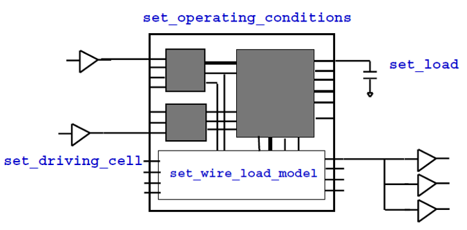
3.1 总论
环境属性中主要有四个参数
- 输入驱动和输入跳变
- 输出负载
- 线负载模型
- 操作条件,即PVT条件
3.2 输入驱动(input drive)和输入跳变(transition)
如果没有设置输入驱动,则DC在计算输入时间的时候,会认为输入跳变为0,这是理想状态下。但为了更好约束时序,需要进行约束,使用指令如下:
1 | |
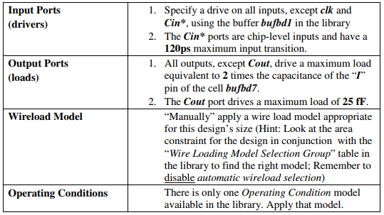
1. LAB解读
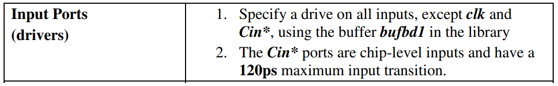
【题目】:用以特定单元
bufbd1,驱动除了clk和Cin*之外的所有输入端口【解析】:使用指令1
【代码】
1
2
3
4
5set_driving_cell -lib_cell bufbd1 -library cb13fs120_tsmc_max \
[remove_from_collection [all_inputs] [get_ports "clk Cin*"]]
# 或
set_driving_cell -lib_cell bufbd1 -library cb13fs120_tsmc_max \
[get_ports "data* sel*"]]
【题目】:
Cin*是一个芯片级的输入端口,最大的输入跳变为120ps【解析】:使用指令2
【代码】
1
2
3set_input_transition 0.12 [get_ports Cin*]
# 如何知道时间单位?
# # 使用指令: report_lib <lib_name> 即可看到对应库的单位
3.3 输出负载(load)
约束设计最多可以负载多大的电容值,使用指令如下
1 | |
1. 常见情况
负载特定值的电容
1
set_load 5 [get_ports OUT1]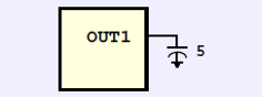
负载相当与某单元某个引脚的电容值
1
2
3set_load [load_of(my_lib/and2a0/A)] [get_ports OUT1]
# 注意: load_of 的使用
# OUT1驱动相当与and2a0单元A引脚的电容值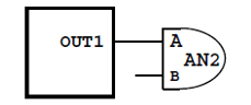
负载相当与多个某单元某个引脚的电容值
1
2
3set_load [expr [load_of(my_lib/inv1a0/A) * 3]] [get_ports OUT1]
# 注意: expr 的使用
# OUT1驱动相当与inv1a0单元A引脚的3倍的电容值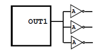
2. LAB解读
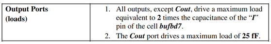
【题目】:除了
Cout,其他输出端口最大可以负载2倍bufbd7的I端口的电容【解析】:除了
Cout端口,其他的输出端口为out1、out2、out3,即其他端口可以使用out*表示 该题目要求,同上文所述的情况3
【代码】
1
set_load [expr 2 * [load_of cb13fs120_tsmc_max/bufbd7/I]] [get_ports out*]
【题目】:
Cout端口,最大可以负载25fF的电容值【解析】:属于情况1
【指令】
1
2
set_load 0.025 [get_ports Cout*]
# 如何看电容“单位”?同上问所述
3.4 线负载模型
1. 如何选定合适的线负载模型
设定线负载模型,需要根据DC综合出来的面积进行设置。
1 | |
部分report_lib.rpt内容如下:
1 | |
关于线负载模型的模式,笔者目前没有用到,不在赘述。
2. LAB解读
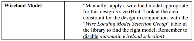
【题目】:根据面积选定合适的线负载模型
【代码】
1 | |
3.5 操作条件(PVT条件)
所谓PVT,即process制程、voltage电压、temperature温度
不同的PVT条件下,DC计算出来的延时是不一样的。通常,制程越慢(ss)、温度越高、电压越低,单元延时越高,如下图
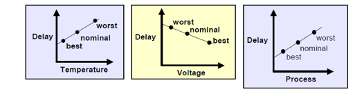
我们希望,芯片在各种各样的PVT情况均可以正常工作。
1. 如何知道有哪些PVT条件
1 | |
部分report_lib.rpt内容如下:
1 | |
可知,PVT条件名为cb13fs120_tsmc_max
2. LAB解读

【题目】:该.db库只有一个PVT条件,设置此PVT条件为当前的PVT条件
【代码】
1 | |
【附录】
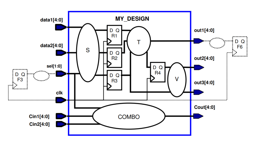
1. 电路图
2. 题干要求
3. 完整指令代码
1 | |
本博客所有文章除特别声明外,均采用 CC BY-SA 4.0 协议 ,转载请注明出处!